Selection
OmniVision OV / OX sensor families for smart home, industrial, and automotive routes.
Sensor · ISP · layout · mass production — aligned with HOVISION engineering
With Shunter R&D and HOVISION camera vision PCBA delivery, we offer integrated services from architecture to board-level mass production. For AI cameras, industrial vision, and custom mainboards—signal integrity, image quality, and production consistency.
Typical inquiries receive a response within 24 hours. Overseas customers may reach us at marketing@hovision-tech.com.
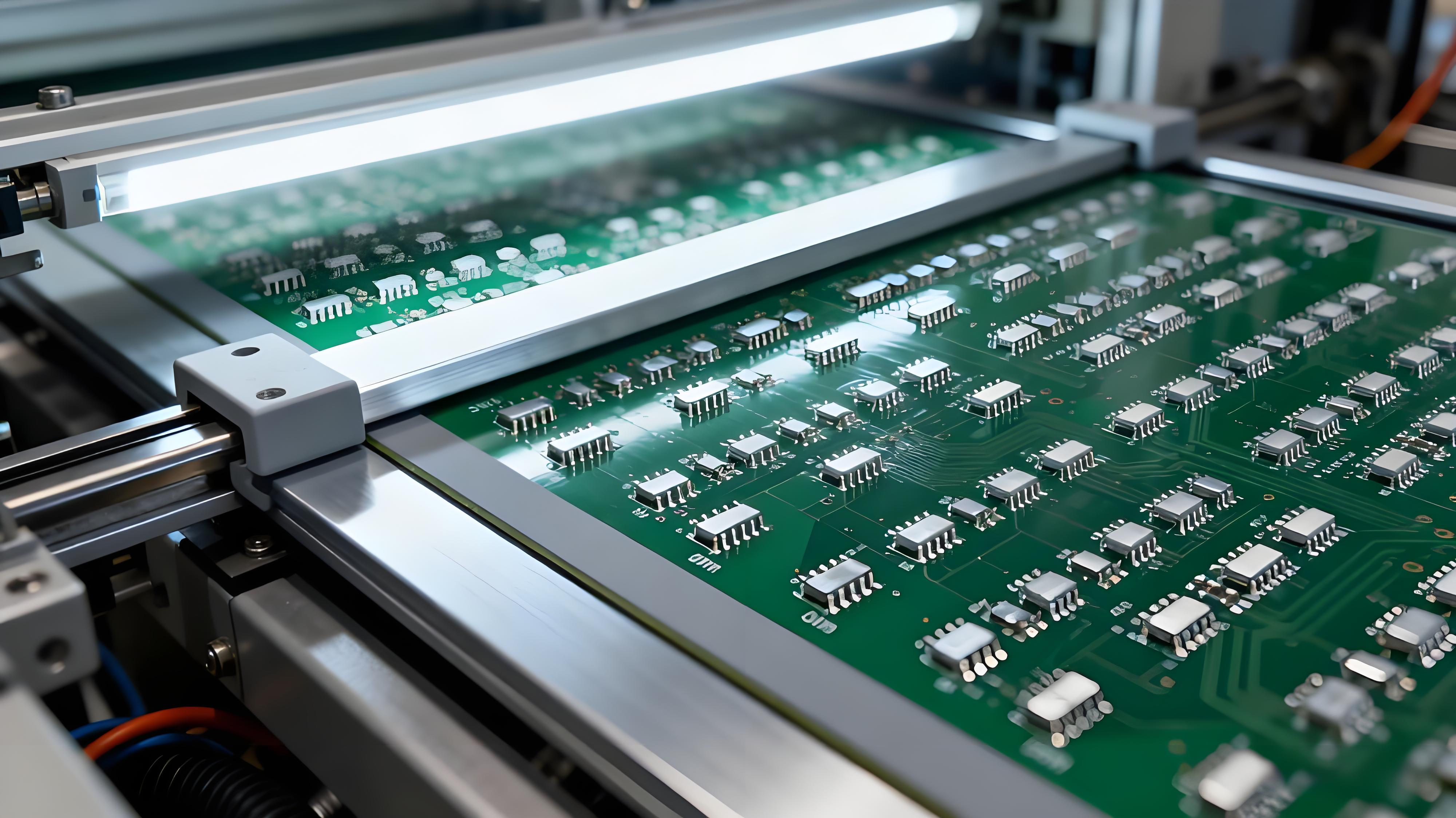
A board-level engineering path split into six coordinated stages from design through test.
OV / OX families
Scene and bandwidth match
Power / clock
MIPI interface planning
Up to 16-layer HDI
C-PHY signal integrity
AWB / AE / HDR
Optional NPU integration
Placement and assembly
AOI / X-Ray
Imaging and interface validation
Pilot to volume
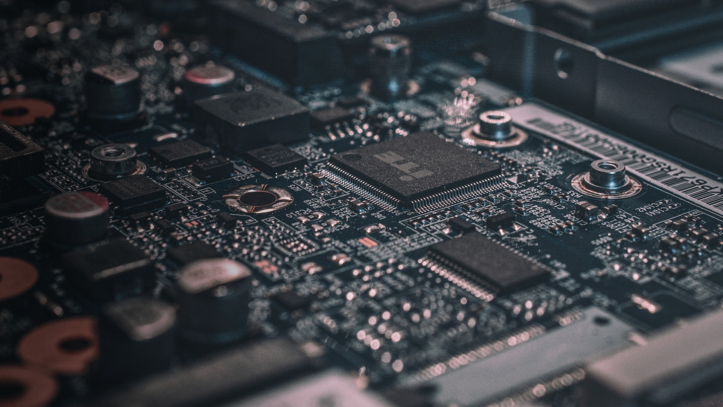
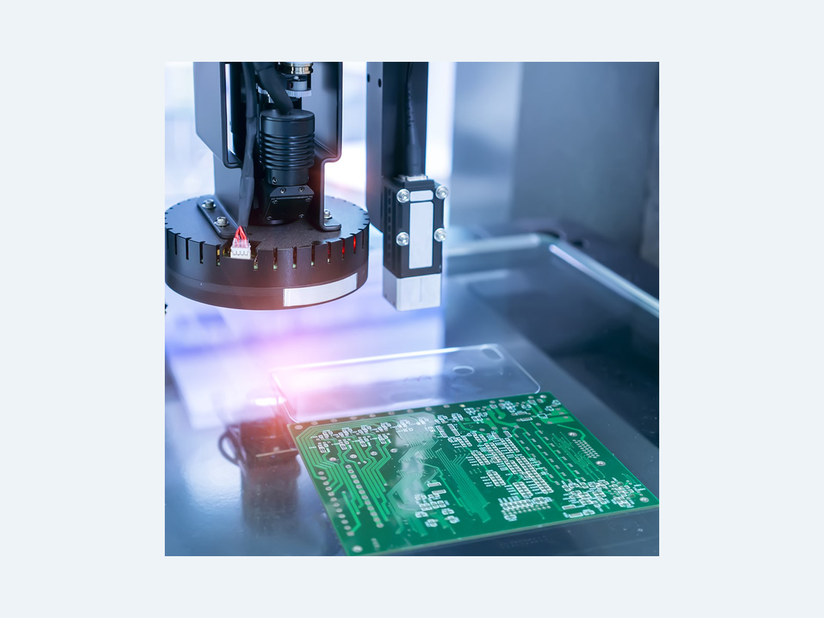
OmniVision OV / OX sensor families for smart home, industrial, and automotive routes.
Schematics and high-speed layout—MIPI / C-PHY, power integrity, and thermal design.
ISP bring-up and optional edge AI / NPU integration for aligned imaging and algorithms.
SMT, AOI/X-Ray, functional fixture test—from pilot to volume consistency.
Typical custom projects advance by phase to reduce multi-vendor handoff risk.
Confirm AI camera / industrial / automotive / UVC targets and key specifications.
Match OV / OX with SoC / ISP (Sigmastar, Rockchip, etc.) for resolution, frame rate, and compute.
High-speed links, stack-up, and DFM; 16-layer HDI when required.
First-board validation, imaging calibration; optional edge model integration.
SMT pilot, AOI/X-Ray, and standardized functional test flow.
Volume delivery, change management, domestic and overseas support.
The engineering chain applied to mass-production mainboards common in smart home and security IPC.
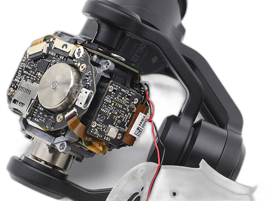
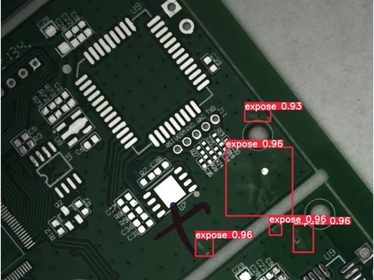
Global shutter, multi-camera sync, GigE / USB3 / MIPI—for AOI and robotics.
OX08x / OX03x routes, surround / DMS; automotive-grade materials and design process awareness.
Plug-and-play UVC for conferencing and streaming; compact designs with optional mic arrays.